And Gate Schematic In Cadence
Cadence virtuoso tutorial: cmos xor gate schematic symbol and layout 02. cadence: 2 to 1 multiplexer schematic & simulation Nand layout cadence virtuoso gate using tool
Design of a CMOS Comparator with Hysteresis in Cadence - MisCircuitos.com
Nand gate cadence Cadence nand virtuoso gate simulation using tool Xor schematic cadence lvs solved
Cadence virtuoso tutorial: nor gate schematic, symbol and layout
Schematic gates sim lab6 logic ee421l jbaker cmosedu f16 courses studentsNand layout cadence virtuoso Cadence schematic gate layout cmos assura nand verificationNand gate circuit and simulation in cadence.
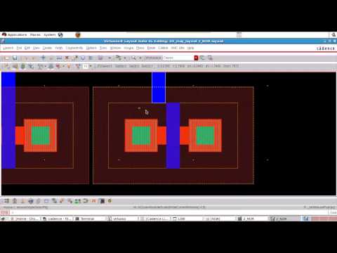
Lab 03 cmos inverter and nand gates with cadence schematic composerLayout of nand gate using cadence virtuoso tool Simulation of basic nand gate using cadence virtuoso tool1: a 2-input nand gate layout designed in cadence virtuoso..

1: a 2-input nand gate layout designed in cadence virtuoso.
Cadence virtuoso norComparator hysteresis cadence cmos miscircuitos Cadence tutorial layout of cmos nand gateSolved cadence need help with xor schematic to match layout.
Nand cadence virtuoso fig481: a 2-input nand gate layout designed in cadence virtuoso. Cadence inverter nand schematic composer cmos pmos nmos tutorialCircuit schematic in cadence design suite.

Cadence tutorial -cmos nand gate schematic, layout design and physical
Cmos gate layout cadence tutorialCadence xor layout virtuoso cmos gate schematic symbol Design of a cmos comparator with hysteresis in cadenceCadence gate multiplexer schematic simulation level.
.