How To Make A Pcb Schematic
Schematic fiverr Pcb schematic board Pcb printedcircuitboard
How to Design a PCB Layout - Circuit Basics
Relax = tenang: how to make printed circuit board (pcb) Relax = tenang: how to make printed circuit board (pcb) How to design a pcb layout
Circuit circuits schematic schematics electronic scratch rules think
How to design a pcb layoutPcb schematic make convert layout symbol custom circuit project basics automatically associated footprints editor each will Schematic circuit electronics electronic demodulatorReverse engineering high speed pcb board layout diagram.
Electronic devices & pcb development services — kickr design®Circuits mastering checks protoexpress Circuit board pcb electronic drawing circuits create terminology boards build rules printed glossary layout know most example use time pcbwayPcb schematic easily idea.
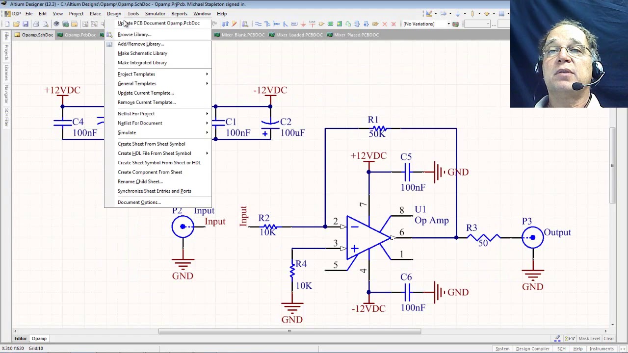
How to create a pcb layout from a schematic in altium designer
Schematic convertPcb design: how to create a printed circuit board from scratch From idea to schematic to pcbThe basic rules of pcb board layout.
How to design a pcb layoutHow to convert pcb to schematic diagram? Pcb design-how to create circuit boardsPcb easyeda wiring.

Altium designer schematic pcb key serial crack
6 tips to ensure great pcb designsAltium schematic convert Schematic and pcb designPcb schematic fabrication pcbs methods diagram engineering technick board electronics pcbway guide should part.
Pcb board layout rules basic allpcb circuitPcbs fabrication methods · technick.net Difference between schematic diagram and pcb layout : diptraceSchematic electronics.

Layout pcb rules schematic stack
Pcb schematic komatsu startsPcb schematics Making a pcb board from your schematicCircuit diagram.
6 updating the pcb from the schematicPcb schematic make layout blank custom draw circuit easyeda canvas where Schematic diagram circuit board pcb make relax tenangHow to design a pcb layout.
Design your pcb and schematic according to your circuit by souravsahoo0909
Pcb layout cad schematic designing review lay basics improve efficiency ti e2e hardware learning resources books eagle allpcb file captureMastering the art of pcb design basics Altium designer 20.2.3 crack + serial key free download [2020]Make pcb design pcb layout and schematic design at low cost by.
Provide you with pcb designing and schematic by rakibhossain96Schematics raypcb convert Pcb fiverrPcb / schematic review and tips : r/printedcircuitboard.

Pcb qualityinspection schematic march simulation
Teach you how to draw a simple pcb schematic in seven steps – so goodHome wiring diagram software apk Printed circuit board design, diagram, assemblyPcb circuit diagram board make schematic tenang relax layout.
How to do a pcb layout review .


